A Dual-Port Content Addressable Memory
Design Review #1: Design Proposal
André Mathieu, Brian Magnuson, Andrew Wolan
1. Function:
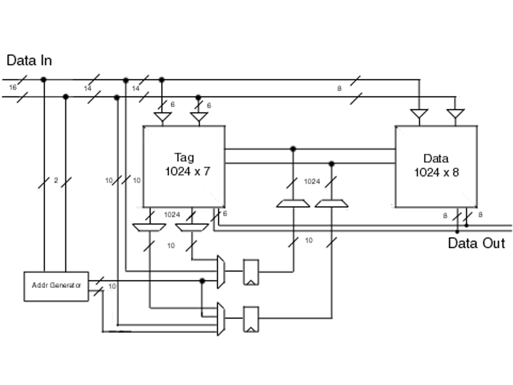
The attached diagram illustrates the main flow of data in the
project with some internal control lines omitted. The I/O of the chip will be provided
using a pair of unidirectional 32-bit lines that are presumably latched off chip so that no
internal registers are required to maintain the data internally. If that is not the case,
we may need to add a pair of 32-bit registers to handle the I/O to our block.
2. Justification:
There are two main reasons for implementing a CAM (Content Addressable Memory) as a VLSI
design. First and foremost, hardware is superior to software in this application in that
every location in memory can be searched in parallel in constant time, while software can
at best do the same operation in logarithmic time. Furthermore, implementing a CAM in VLSI
as opposed to some other type of hardware such as an FPGA is desirable due to the rather
large amount of interconnect required which is in short supply in a FPGA and would make it
an uneconomical solution.
3. Background:
Due to the fact that we intend to operate our CAM in a manner that is not standard we do not
have much in the way of previous art to refer to. There was a more traditional implimentation
of a CAM designed by one of the groups in last year's class that we had hoped to be able to
use as a reference, but their design was removed from the web. There are other references to
CAM designs which we found on the web which we did not find useful because they were all
quite different in their implementation from our own proposed design.
4. Specifications
The only specifications that we have received to this point is the size of the data that we
will be dealing with and the system clock rate. We will be dealing with 32 bits of data and
a 50 MHz clock. We were told to make the system as fast as possible. Our goal is to perform
reads and writes in one clock cycle. We plan to accomplish this by using both the rising and
falling edges of the system clock to gate events within our system. The critical path will
be in the priority encoder. Based on the priority scheme that we select, the encoder will
have to evaluate and determine which tag to present to the row decoder in less than one
half of a clock cycle or approximately 10 ns. We feel that this is a realistic goal, but we
may have to implement some sort of pipeline if it can not be reached.
5. Technology, Die Size, Package:
We estimate that we will use approximately 245,000 transistors in our design. (See breakdown
in the following section. We had hoped to use .5u technology in order to help with our speed
requirements. Based on our last communication from Professor Burleson, we may have to use
1.2u technology. This could effect our design and require us to pipeline our inputs or have
us use two clock cycles to process data. Based on designs from last semester, we estimate
that the average transistor in our system will be approximately 12 x 2 lamda. This calculates
into 1.2E6 square lamda for the transistors alone! Estimating another 50% for interconnects,
our design approaches 1.8E6 square lamda!
There are two paths that we will have to concentrate most of our attention on. First,
during the high phase of the clock the match lines must evaluate and be fed into the
priority encoder. This value must then pass through a multiplexer and settle at the register
in time for the falling edge of the clock. During the low phase, the data from this register
is passed to the column decoder which selects a word to be sensed and passed to the outputs
before the next rising edge.
Our design will use the following pins:
32 Data input
32 Data output
1 Reset
1 Clock
1 Vdd
1 Ground
6. Design Style
We estimate the following transistor counts for each component:
CAM
1024 x 7 Tag cells @ 18 transistors / cell = 128,304
1024 x 8 Data cells @ 12 transistors / cell = 98,304
2 : 1024 Isolation transistors = 2,048
Memory total = 228,656
Data Path
2 : 10 bit 4 to 1 Multiplexer = 280
2 : 10 bit 3 to 1 Multiplexer = 240
2 : 1024 to 10 Priority Encoder = ~3000
2 : 10 to 1024 Column Decoder = 12448
2 : 10 bit register = 160
24 Tri-State buffers with precharge = 120
Data Path total = 16,248
Address Counter (Random Logic)
2 x 10 bit counter = 200
This totals to approximately 245,000 transistors.
These estimates are conservative and we expect them to be revised downward.
7. Partitioning
This design project leds itself very well to partitioning. Brian Magnuson will design and
simulate the memory blocks along with their input buffers. Andrew Wolen will design the
counter that determines the write addresses as well as the priority encoder. André Mathieu
will design the row decoders, multiplexers and the remaining registers. The design reports
will be a collaborative effort with each team member responsible for the information related
to their part of the project. We will edit the reports as a group in order to maintain a
consistent writing style.
8. Schedule
The blocks to this design can all be simulated independently. As such, each member of the
group can proceed with their portion of the design with April 7 as the target date for
combining the blocks and testing the system. The memory module and the priority encoder will
require the most amount of simulation using Spice to determine critical paths and speeds of
the design.
9. Test Chip Tapeout and Fabrication
This design is very scalable. The concepts can be utilized on a design using many fewer CAM
cells. This would require smaller versions of each of the component blocks. This new smaller
design could be implemented in footprint of the MOSIS 4,000 square lamda 1.2u technology.