Control Block:
State Transitiion Table:
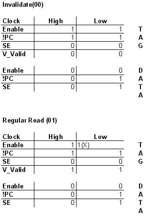
(The X implies a "don't care" state.)
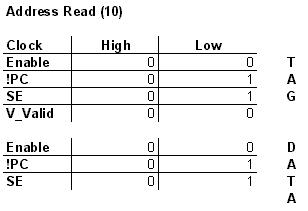
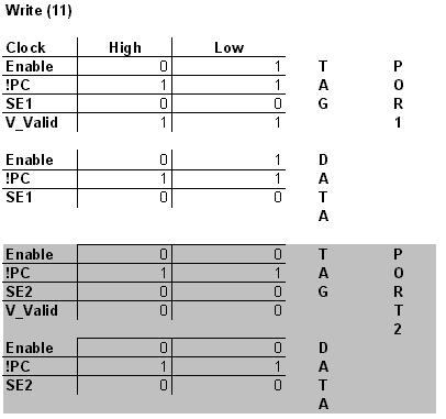
Information:
The control block is comprised solely of combination logic. (IE, no state machine was needed.) It's job is to drive the control signals for the tag and data memories. To keep the design on the control block modular, one control block is needed per port. (Hence, two control blocks are needed since our memory is dual-ported.)
A description of the control signals is as follows:
AB = opcode
C = clock
Tag Memory
EN, !EN = enable singles
!PC = pre-charge
SE = sense enable
V_Valid = valid bit value
Data Memory
D_EN, !D_EN = enable singles
D_!PC = pre-charge
D_SE = sense enable
* Note: The input of port 2 of the data cell is not used. Thus, EN and !EN inputs of the buffer are tied to GND and Vdd respectively instead of to the control block.
This allows us to impliment the "dual port" control of the write operation without the need of extra logic.
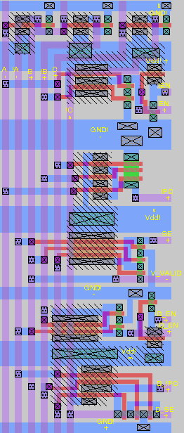
VLSI Layout
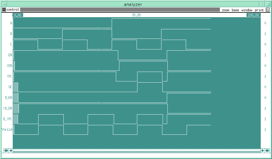
IRSIM Simulation
Specs:
Speed: 3ns max
Size: 265 x 105 lambda
# transisters: 72
# drawn trans: 36
replication factor: 2x
active area vs. routing area: 3436/24389 = 10%
total area/block: 27825 lambda sq.
area vs # trans: 386.46 lambda sq / tran.
power consumption: 27.1 E -12 W
design time: 36 hrs.
Modifications:
None.
Downloads:
Control Block Layout