Data Sheet for the Priority Based Dual-Port Content Addressable Memory (PB CAM)
Designed by TeamX - André Mathieu, Brian Magnuson, Andrew Wolan
http://teamx.emulationzone.org
Released 5/12/2000
Discription:
The PB-CAM allows for the storage of 32 8-bit values. The values are stored not only by a given tag, but on a priority level as well. The priority of a tag is used to select between two or locations with the same tag value. The priority level corresponds to the memory address in the CAM, where location 0 has a the highest priority and location 31 has the lowest.
Data is entered or read from the CAM using one of the 4 op codes below.
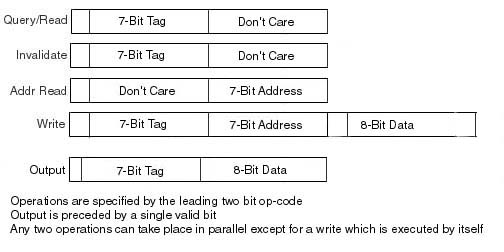
The dual port nature of the PB-CAM allows for the 2 simultaneous reads at a time. 2 invalidate instructions can be executed in parallel as well. However, due to the size of the fields for a write instruction, only one write can be presented at a time.
Pin Layout:
	        ------------
  Data_in1      |1        68| Vdd
  Data_in2    	|2        67| Data_out32
  Data_in3      |3        66| Data_out31
  Data_in4      |4        65| Data_out30
		.           .
	        .           .
	        .           .
  Data_in32     |32       37| Data_out2
  Reset         |33       36| Data_out1
  GND           |34       35| Clock
                ------------
Engineering Notes:
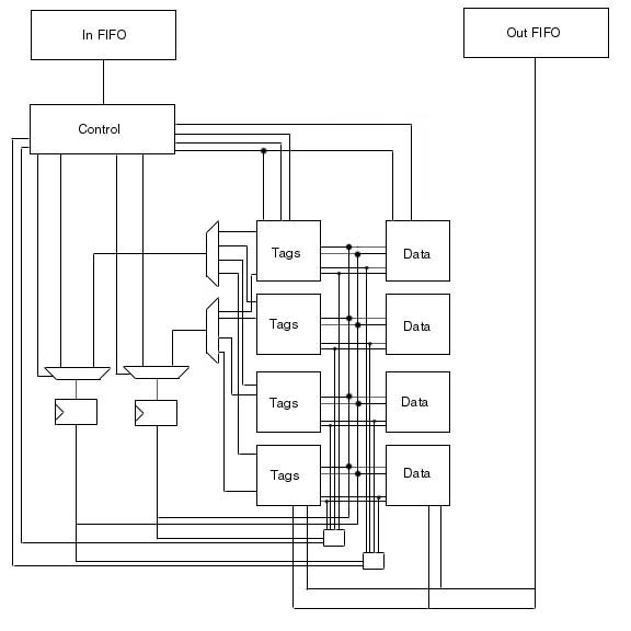
Block Diagram
Technology - 1.2u
Number of transistors - 7170
Clock Rate = 16.666 Mhz
Power Consumption: 10.7 E -9 W
Designed using Magic, IRSIM and CazM on SUN Ultra Workstations
Design Time: A semester (14 weeks)
Componets of this project can be viewed at our home page, or directly by visiting
http://teamx.emulationzone.org/menuA.htm. There, you will find schematics, simulation plots, statics and
even the VLSI layouts in Magic format.
Links:
Course Homepage
Copyright(c) 2000 André Mathieu, Brian Magnuson, Andrew Wolan